Please select your location and preferred language where available.
Toshiba Now Shipping Samples of 64-Layer, 512Gb 3D Flash Memory
Expands Lineup with Largest Capacity BiCS FLASH Device, Enabling 1-Terabyte Single Chip
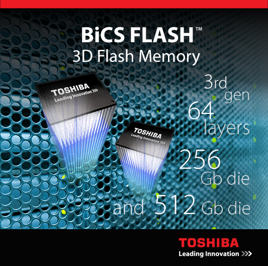
IRVINE, Calif., February 24, 2017 -- Toshiba America Electronic Components, Inc. (TAEC)* today announced that it has added a 512 gigabit (Gb)1 (64 gigabyte), 64-layer device with 3-bit-per-cell triple-level cell (TLC) technology to its industry-leading BiCS FLASH™ product line. This technology will enable a 1-terabyte (TB) chip solution. BiCS FLASH is a three-dimensional (3D) flash memory stacked cell structure2 and is suitable for applications that require high capacity and performance, such as enterprise and consumer solid state drives, including Toshiba’s own SSD portfolio. Sample shipments of the new 512Gb devices have begun, with mass production scheduled for the second half of 2017.
As a 3D flash memory leader, Toshiba continues to refine its BiCS FLASH offerings. The next milestone on its BiCS FLASH development roadmap will feature the industry’s largest capacity3, a 1TB product with a 16-die stacked architecture, in a single package. Plans call for sample shipments to commence in April of this year.
Toshiba’s new 512Gb BiCS FLASH device is based on its cutting-edge, third generation, 64-layer stacking process that realizes a 65 percent larger capacity per unit chip size than the company’s 48-layer, 256Gb (32 gigabyte) device. This increases memory capacity per silicon wafer and leads to a reduction of cost-per-bit.
In addition to the new 512Gb device, Toshiba’s BiCS FLASH lineup also includes a 64-layer 256Gb (32 gigabyte) offering, which is currently in mass production. According to Scott Nelson, senior vice president of TAEC’s memory business unit, “The introduction of our third generation BiCS FLASH coupled with the industry’s largest 1TB chip solution strongly reinforces Toshiba’s flash leadership position. These innovations underline our commitment to developing leading-edge memory solutions, and we will continue to advance our 3D technology to meet the ever-increasing storage market demand.”
In support of this commitment, Toshiba recently announced that construction has begun on a new state-of-the-art semiconductor fabrication facility, Fab 6, and a new memory-focused R&D Center, at Yokkaichi Operations in Mie Prefecture, Japan. Fab 6 will be dedicated to the production of BiCS FLASH.
For more information, please visit toshiba.com/technologymoves, read the TAEC Memory Blog and follow the company on Facebook and Twitter.
*About TAEC
Through proven commitment, lasting relationships and advanced, reliable electronic components, Toshiba enables its customers to create market-leading designs. Toshiba is the heartbeat within product breakthroughs from OEMs, ODMs, CMs, VARs, distributors and fabless chip companies worldwide. A committed electronic components leader, Toshiba designs and manufactures high-quality flash memory-based storage solutions, solid state drives (SSDs), hard disk drives (HDDs), solid state hybrid drives (SSHDs), discrete devices, custom SoCs/ASICs, imaging products, microcontrollers, wireless components, mobile peripheral devices, and advanced materials that make possible today’s leading smartphones, tablets, cameras, medical devices, automotive electronics, industrial applications, enterprise solutions and more.
Toshiba America Electronic Components, Inc. is an independent operating company owned by Toshiba America, Inc., a subsidiary of Toshiba Corporation, Japan’s largest semiconductor, solid state drive and hard disk drive manufacturer and the world’s seventh largest semiconductor manufacturer (Gartner, 2015 Worldwide Semiconductor Revenue, January, 2016). Founded in Tokyo in 1875, Toshiba is at the heart of a global network of over 550 consolidated companies employing over 188,000 people worldwide (as of March 31, 2016). Visit Toshiba's web site at http://toshiba.semicon-storage.com.
1 Product density is identified based on the density of memory chip(s) within the Product, not the amount of memory capacity available for data storage by the end user. Consumer-usable capacity will be less due to overhead data areas, formatting, bad blocks, and other constraints, and may also vary based on the host device and application. For details, please refer to applicable product specifications.
2 A structure stacking Flash memory cells vertically on a silicon substrate to realize significant density improvements over planar NAND Flash memory, where cells are formed on the silicon substrate.
3 As of February 22, 2017. Toshiba survey.
BiCS FLASH is a trademark of Toshiba Corporation.
- The products are labeled based on the memory chip(s) it contains, not the amount of memory capacity available for data storage by the end user. Part of the capacity is reserved for device management. Please refer to the data sheet or your local Toshiba sales representative. (For purposes of measuring memory capacity in this context, 1GB = 1,073,741,824 bytes).
- Information in this press release, including product pricing and specifications, content of services, and contact information is current and believed to be accurate on the date of the announcement, but is subject to change without prior notice. Technical and application information contained here is subject to the most recent applicable Toshiba product specifications.