Please select your location and preferred language where available.
Toshiba Memory America Introduces Next-Gen Serial Interface NAND
New NAND Flash Memory Products for Embedded Applications Support High-Speed Data Transfers, Offer Performance and Density Improvements
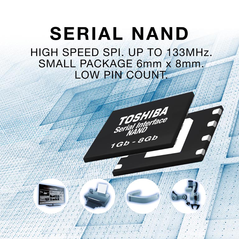
SAN JOSE, Calif., September 26, 2019 – Toshiba Memory America, Inc. (TMA), the U.S.-based subsidiary of Toshiba Memory Corporation, today announced the launch of a new family of SLC NAND flash memory products for embedded applications. Compatible with the widely used Serial Peripheral Interface (SPI), Toshiba Memory’s second-generation Serial Interface NAND can be used in a wide range of consumer and industrial applications that require high-speed data transfers, including flat screen TVs, printers, wearable devices, and robots.
The new products bring improved speed (from 104MHz to 133MHz) over Toshiba Memory’s previous generation and include a new command for loading data for programming in 4-bit (QSPI) mode. The addition of an 8-gigabit (Gb) device also brings improved NAND density to the new generation of products. The second-generation Serial Interface NAND family consists of eight products and features power supply voltages of 2.70 to 3.60V and 1.70 to 1.95V. Samples are available now and mass production is scheduled to begin in October.
NOR flash memory has commonly been used in embedded applications for consumer and industrial devices. However, in order to support the new, enhanced features found in embedded devices, larger memory densities are needed. This is especially true in IoT and communications applications, where device miniaturization means that fast, large-capacity flash memory is required – in the smallest package possible. Additionally, microcontroller manufacturers are moving away from the high-pin-count parallel address/data bus in favor of lower-pin-count interfaces, making an alternative to NOR even more important.
"SLC NAND was the very first NAND flash that was developed – and it is still widely used today,” noted Brian Kumagai, director of business development Toshiba Memory America, Inc. “At Toshiba Memory, not only do we remain committed to supporting SLC – we continue to innovate to enable new classes of applications. With our new second-generation Serial Interface NAND, we’re providing an excellent NOR flash alternative, giving users a higher density, more cost-effective solution.”
Product Lineup
| Part Number | Density |
I/O | Voltage | Package | Mass Production |
|---|---|---|---|---|---|
| TC58CVG0S3HRAIJ | 1Gb | x1, x2, x4 | 3.3V | 8pin WSON1 (6mm x 8mm) |
Oct. 2019 |
| TC58CYG0S3HRAIJ | 1.8V | Oct. 2019 | |||
| TC58CVG1S3HRAIJ | 2Gb | 3.3V | Oct. 2019 | ||
| TC58CYG1S3HRAIJ | 1.8V | Oct. 2019 | |||
| TC58CVG2S0HRAIJ | 4Gb | 3.3V | Oct. 2019 | ||
| TC58CYG2S0HRAIJ | 1.8V | Oct. 2019 | |||
| TH58CVG3S0HRAIJ | 8Gb | 3.3V | Dec. 2019 | ||
| TH58CYG3S0HRAIJ | 1.8V | Dec. 2019 |
Key Features
|
Density |
1Gb, 2Gb, 4Gb, 8Gb |
|---|---|
|
Page Sizes |
2KByte (1Gb, 2Gb), 4KByte (4Gb, 8Gb) |
|
Interface |
Serial Peripheral Interface Mode 0, Mode 3 |
|
Power Supply |
2.70 to 3.60V, 1.70 to 1.95V |
|
Operating |
-40 oC to 85 oC |
|
Features |
|
For more information, please visit business.toshiba-memory.com.
Notes:
1 WSON: Very-Very thin Small Outline No Lead Package
All company names, product names and service names may be trademarks of their respective companies. In every mention of a Toshiba Memory product: Product density is identified based on the density of memory chip(s) within the Product, not the amount of memory capacity available for data storage by the end user. Consumer-usable capacity will be less due to overhead data areas, formatting, bad blocks, and other constraints, and may also vary based on the host device and application. For details, please refer to applicable product specifications. The definition of 1Gb = 2^30 bits = 1,073,741,824 bits. The definition of 1GB = 2^30 bytes = 1,073,741,824 bytes.
About Toshiba Memory America, Inc.
Toshiba Memory America, Inc. is the U.S.-based subsidiary of Toshiba Memory Corporation, a leading worldwide supplier of flash memory and solid state drives (SSDs). From the invention of flash memory to today’s breakthrough 96-layer BiCS FLASH™ technology, Toshiba Memory continues to lead innovation and move the industry forward. For more information, please visit business.toshiba-memory.com and follow us on social media. Toshiba Memory will officially change its name to Kioxia on October 1, 2019.
- Information in this press release, including product pricing and specifications, content of services, and contact information is current and believed to be accurate on the date of the announcement, but is subject to change without prior notice. Technical and application information contained here is subject to the most recent applicable Toshiba Memory product specifications.
