Please select your location and preferred language where available.
Innovative Technologies That Pave Ways to Higher Capacity
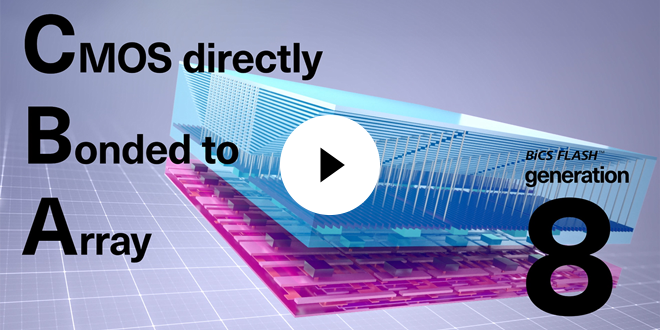
Underpinning the major enhancements of current generation BiCS FLASH™ products are several breakthrough technology innovations. Improvements in density, performance and power efficiency were achieved through advances in flash memory engineering design and assembly processes. Explore how CMOS directly Bonded to Array (CBA) , On Pitch Select Gate (OPS) and 32-die memory assembly are delivering the future of 3D flash memory.
Technologies In the Front-End Process
Interview
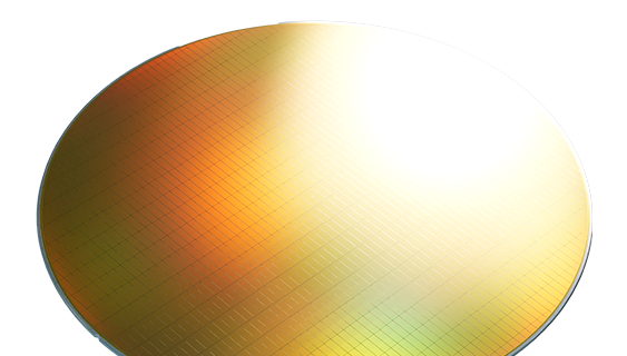
High-density 3D flash memory using high-precision wafer bonding brings new value to storage
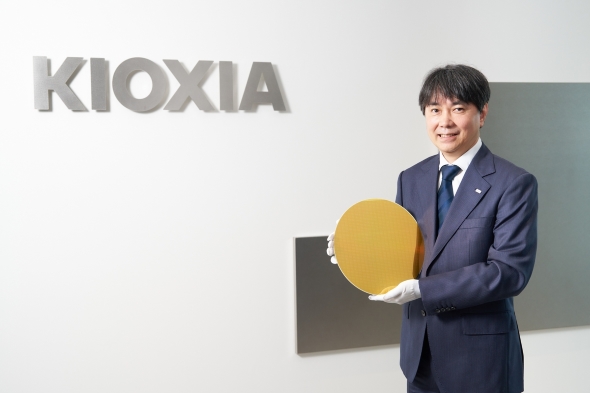
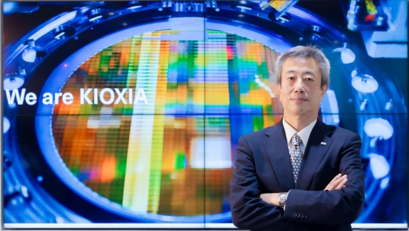
In recent years, flash memory manufacturers have focused primarily on developing technologies to increase the number of layers of memory cells and increase memory density. Each time a new generation of flash memory is released, the number of layers increases with some products boasting more than 200 layers. However, as Atsushi Inoue, Vice President of Memory Division at KIOXIA, explained, "Increasing the layers of memory cells is only one way of increasing capacity and memory density, and we are not exclusively preoccupied with the number of layers."
Assembly Technology In the Back-End Process
Interview
Leading the AI Evolution with Innovative 2mm Flash Memory Assembly Technology
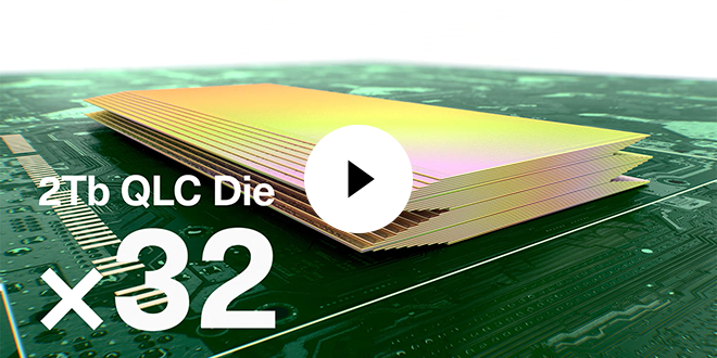
32 memory dies assembled into a single package
The rapid growth of AI has accelerated demand for flash memory capacity. KIOXIA has successfully developed large-capacity 8 TB (terabyte) flash memory by assembling 32 pieces of 2 Tb (terabit) memory dies into a package less than 2 mm in height. This achievement was made possible with advanced assembly process technologies, including the technology for making wafers as thin as possible.
Fundamentals of BiCS FLASH™ Technologies Common to All Generations
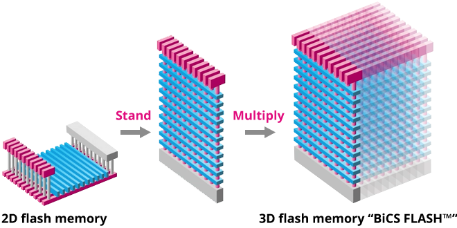
BiCS FLASH™ 3D flash memory vertically stacks memory cells, significantly increasing storage density. This skyscraper-like architecture overcomes the limits of 2D (planar) flash memory, which arranges cells in a side-by-side format. Increasing the distance between cells reduces cell-to-cell interference, enabling better density, performance, and power efficiency compared to 2D flash memory.
TLC (Triple Level Cell) and QLC (Quadruple Level Cell) Technology
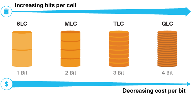
BiCS FLASH™ 3D flash memory product lineup includes both 3-bit-per-cell (TLC) and 4-bit-per-cell (QLC) technology. QLC technology significantly expands capacity by pushing the bit count for data per memory cell from three to four. A capacity of 4 terabyte (TB) can be achieved in a single package using BiCS FLASH™ QLC technology in a 16-die stacked architecture.
KIOXIA was one of the first industry players to envision and prepare for the successful migration of SLC technology to MLC, from MLC to TLC, and from TLC to QLC.
KIOXIA QLC technology is ideal for applications requiring high density, lower cost storage solutions. Today’s QLC reduces the footprint with the highest density available in a single package enabling storage solution to scale.

Products by Applications
Whether it’s automotive applications or compact high performance-oriented PCs or cloud server and hyperscale data center deployments, by delivering advanced high performance, high density, low power, low latency, reliability and more—KIOXIA memory and storage solutions enable the success of emerging applications and allow existing technologies to reach their expected potential.
Support

Please contact us if you have any technical questions, requests for materials, are interested in samples or purchases of business products (Memory, SSD), etc.

In 2007, KIOXIA announced the world‘s first 3D flash memory technology. Presenting our cutting-edge technologies, along with the key points of innovation and our efforts toward further increases in capacity.

KIOXIA invented the world’s first NAND flash memory in 1987. This is an explanation of the structure of flash memory and the mechanism of data storage.
